
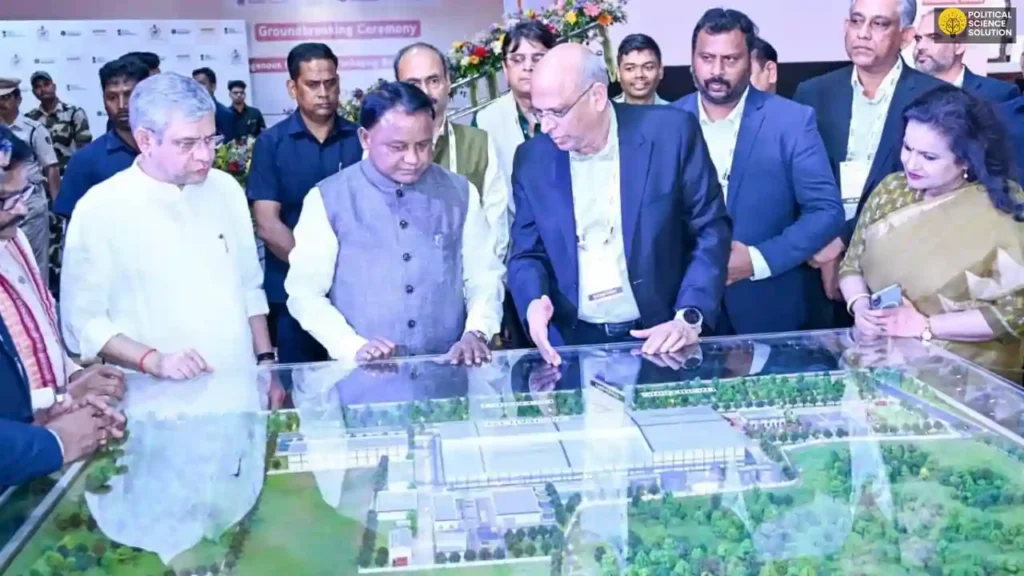
New Delhi: Odisha has taken a decisive step into the semiconductor era with the groundbreaking of India’s first advanced 3D glass substrate-based semiconductor packaging facility at Info Valley, Bhubaneswar. Chief Minister Mohan Charan Majhi and Union Electronics and IT Minister Ashwini Vaishnaw jointly laid the foundation stone on April 20, 2026, for this strategically important project.
Project Overview and Key Details
The facility is being developed by US-based 3D Glass Solutions Inc. (3DGS) through its wholly owned Indian subsidiary, Heterogeneous Integration Packaging Solutions Pvt Ltd. The project carries an investment of approximately ₹1,934 crore to ₹1,943 crore (rounded near ₹2,000 crore in some references) and has received approval under the India Semiconductor Mission (ISM).
It will operate as a fully vertically integrated ATMP (Assembly, Testing, Marking, and Packaging) unit. Intel is among the key funders, and Intel CEO Lip-Bu Tan joined the ceremony virtually, reflecting strong global investor interest.
Production Capacity and Timeline
Upon full operation, the plant will produce 69,600 glass panel substrates, 50 million assembled units, and around 13,200 advanced 3D heterogeneous integration (3DHI) modules annually. Commercial production is scheduled to begin by August 2028, with full-scale operations targeted for 2030. The project is expected to generate approximately 2,500 direct and indirect jobs for engineering graduates, diploma holders, and ITI-trained professionals.
Technological Breakthrough: 3D Glass Substrate Packaging
This unit introduces India’s first commercial-scale use of advanced 3D glass semiconductor technology. It employs specialised glass substrates and glass interposers instead of traditional silicon for packaging. Glass offers superior radio frequency performance, significantly lower electrical loss, better thermal stability, and higher integration density compared to conventional organic or silicon-based packaging.
The technology enables three-dimensional heterogeneous integration (3DHI), allowing multiple chips and passive components to be embedded efficiently. This makes the facility critical for manufacturing high-performance chips required in artificial intelligence, machine learning, 5G/6G communications, data centres, defence electronics, aerospace systems, and high-performance computing.
Strategic Importance for India’s Semiconductor Ecosystem
India currently imports over 90% of its semiconductor needs, while globally, around 70% of semiconductor manufacturing capacity remains concentrated in South Korea, Taiwan, China, the United States, and Japan. This project directly addresses supply chain vulnerabilities exposed during the Covid-19 pandemic and the Russia-Ukraine conflict.
By localising advanced packaging capabilities, India strengthens economic security, reduces import dependence, and supports emerging high-tech sectors. The plant marks a vital addition to the domestic value chain, moving beyond assembly toward sophisticated 3D integration technology.
National Initiatives Driving the Project
The foundation stone laying aligns with the India Semiconductor Mission (ISM) and Semicon India Programme, which aim to build a complete semiconductor and display ecosystem. Supporting efforts include the Chips to Start-up (C2S) Programme, AICTE curriculum reforms introducing specialised semiconductor courses, and the promotion of indigenous microprocessor technologies such as SHAKTI, VIKRAM, and DHRUV64 under the Digital India RISC-V Programme.
Global collaborations like the India-US Initiative on Critical and Emerging Technology (iCET) and the Pax Silica Initiative further strengthen the ecosystem. Central schemes such as the Scheme for Promotion of Manufacturing of Electronic Components and Semiconductors (SPECS) and Electronics Components Manufacturing Scheme (ECMS) provide additional policy support. Several states, including Gujarat with its Semiconductor Policy 2022–27, have also rolled out attractive incentives.
Odisha’s Emergence as a Semiconductor Hub
Odisha has become the only state in India to host both a compound semiconductor fabrication unit and a 3D glass substrate packaging facility. The SiCSem Private Limited project, in partnership with UK-based Clas-SiC Wafer Fab Ltd., is already under construction at the same Info Valley campus. It targets 60,000 silicon carbide wafers and 96 million packaged units per year for electric vehicles, railways, defence, and renewable energy.
Union Minister Ashwini Vaishnaw described the day as historic for Odisha, noting the state’s shift from traditional mining, metal, and power industries to high-tech electronics and IT sectors. He announced plans to double the plant’s capacity after the successful completion of the first phase. Chief Minister Mohan Charan Majhi termed the project a milestone that positions Odisha as a preferred destination for global technology investments from companies like Intel, Lockheed Martin, and Applied Materials.
State IT Minister Mukesh Mahaling highlighted the role of Odisha’s new IT, AI, GCC, and Semiconductor Policies 2025 in attracting further investment and fostering innovation. The state government is prioritising skill development programmes, including financial support for students, to prepare a ready workforce for the semiconductor industry.
Broader Impact on Employment and Economy
Beyond direct jobs, the project is expected to stimulate ancillary industries, research activities, and infrastructure development. It complements Odisha’s larger industrial push, which has attracted projects worth ₹2.8 lakh crore and generated two lakh jobs since the current government took charge. The semiconductor initiative reinforces the state’s transition from a resource-based to a technology-driven economy, supported by improved railway and connectivity infrastructure.
National Context and Future Outlook
The Union Cabinet approved both Odisha projects in 2025 as part of a nationwide push that has cleared 10 semiconductor initiatives with total investments exceeding ₹1.6 lakh crore. This Bhubaneswar facility strengthens India’s ambition to become a global hub for electronics manufacturing and design.
Industry experts believe the glass substrate technology will provide a competitive edge in thermal management and signal integrity—key requirements for AI-grade chips and next-generation defence systems. As the plant progresses toward 2028 production, it is set to enhance India’s technological self-reliance and reduce exposure to global chip shortages.
The successful implementation of this project, combined with ongoing talent development and policy support, will play a crucial role in building a resilient and innovative semiconductor ecosystem. Odisha’s proactive approach positions it as a rising leader in India’s high-tech manufacturing landscape, contributing meaningfully to the vision of Atmanirbhar Bharat.
Frequently Asked Questions (FAQs)
1. What is India’s first advanced 3D semiconductor packaging unit and where is it being set up?
India’s first advanced 3D glass substrate semiconductor packaging unit is a vertically integrated ATMP (Assembly, Testing, Marking, and Packaging) facility. It is being established at Info Valley in Bhubaneswar, Odisha. The project is promoted by US-based 3D Glass Solutions Inc. through its Indian subsidiary and received approval under the India Semiconductor Mission.
2. What is the investment, capacity, and expected timeline of the Bhubaneswar 3D glass chip packaging plant?
The project involves an investment of approximately ₹1,934–2,000 crore. Once operational, it will produce 69,600 glass panel substrates, 50 million assembled units, and 13,200 advanced 3DHI modules annually. Commercial production is expected to start by August 2028, with full-scale operations targeted for 2030. It is projected to create around 2,500 direct and indirect jobs.
3. Why is glass substrate technology important compared to traditional silicon packaging?
Glass substrate technology offers superior radio frequency performance, lower electrical loss, better thermal stability, and higher integration density than conventional silicon or organic packaging. It enables advanced 3D heterogeneous integration (3DHI), making it highly suitable for high-performance applications in AI, 5G/6G, defence, data centres, and high-performance computing.
4. How does this project benefit India’s semiconductor ambitions and Odisha’s economy?
The facility will help reduce India’s over 90% dependence on imported semiconductors and strengthen the domestic supply chain. For Odisha, it marks a shift from traditional mining and metal industries to high-tech electronics manufacturing. It positions the state as the only one in India hosting both a silicon carbide fab and a 3D glass packaging unit, while generating significant employment and attracting further global investments.
5. Which sectors will benefit from the chips packaged at this Bhubaneswar facility?
The plant will supply advanced packaged chips for critical sectors including Artificial Intelligence (AI), machine learning, 5G and 6G communications, defence electronics, aerospace, data centres, high-performance computing, and advanced digital systems. This will enhance India’s self-reliance in strategic and emerging technologies.

